|
|
Bachelor's Degree in Telecommunications Systems and in Network Engineering |
|
|
|
|||||
Chapter 2 problems |
- D2.17 - |
Shower stall automation (FPGA-VHDL) |
|||
|
|
|||||
1. Specifications
In a gym and fitness centre, there are some shower stalls like the one represented in Fig. 1 that have to be automated to generate cycles of contrasting hot (48 °C), warm (26°C) and cold (4°C) water sprays simply clicking a single start push button (SB). After clicking the SB, initially warm water flows for 50 s (H = C = ‘1’), then hot water (H = ‘1’, C = ‘0’) for 10 s, and thirdly cold water (H = ‘0’, C = ‘1’) for 20 s, and this cycle is repeated another time; finally, the system goes idle (H = C = ‘0’) to wait for another user service. During the operation the R_LED turns on and the water solenoid valve (SV) is on. Let us design the digital control system connected to the valves’ power driver (Chip5) using an FPGA chip and organising several design steps.
The same project designed programming a μC is in D3.17.
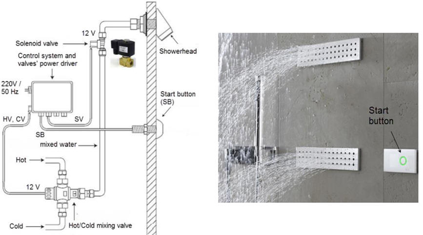 |
| Fig 1. Symbol for the proposed entity. |
We conceive an internal architecture as shown in Fig.2.
1. Explain the function of the circuit Chip1, why it is required for conditioning the start button external signal.
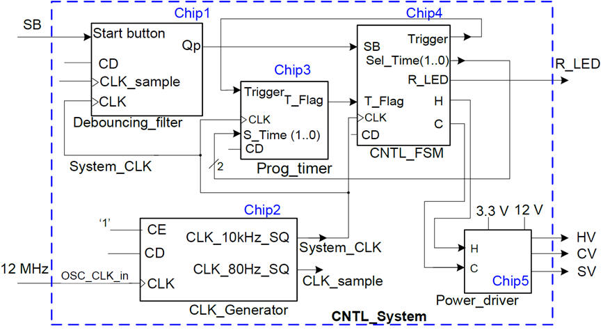 |
| Fig 2. Internal architecture of the proposed control system as a dedicated processor. |
With respect to the Chip4:
2. Draw the state diagram of the application explaining both, state transitions and outputs in each state.
3. Draw an example of a timing diagram.
4. Draw the architecture of a FSM for the Chip4 explaining where all the inputs and outputs are connected.
5. Draw the CC2 truth table and its flowchart interpretation, so that it can be coded in VHDL in the usual CSD style.
6. Draw the CC1 truth table and its flowchart interpretation, so that it can be coded in VHDL in the usual CSD style.
7. Draw the internal circuit of the state register. How many bits and DFF (data-type flip-flops) will be used if the states are coded in one-hot?
With respect to the Chip3:
8. Explain the internal architecture, components and the number of VHDL files of the Prog_Timer project.
With respect to the Chip2:
9. Deduce and explain the internal architecture, the number of VHDL files and names of the CLK_Generator project.
10. We have measured by means of a gate-level VHDL simulation for the target CPLD/FPGA where the circuit is synthesised, a worst-case CLK to output propagation delay (tCO) of 6.3 ns. Thus, which is the maximum OSC_CLK_in frequency and so the minimum pulse duration?
| Home Term 23/24-Q2 Contact Products Electronic devices and companies Software Books Magazines Instruments DEE Library EETAC DEEL |

|
|
| Web activa des de 09/2001, @ F. J. Robert, J. Jordana. Web editat amb Microsoft Expression Web 4. El contingut és un complement als materials d'estudi del curs Circuits i Sistemes Digitals disponibles al campus digital Atenea. Llicència:Reconeixement 4.0 Internacional de Creative Commons |